What is Atomic Force Microscope (AFM)? The Atomic Force Microscope (AFM) is a high-resolution scanning probe microscopy technique, jointly invented by Gerd Binnig, Heinrich Rohrer, and Calvin Quate in 1986. AFM operates by measuring the interaction forces between a sharp probe mounted on a microcantilever and the surface of a sample. This method allows for the detection of surface topography and physical properties of the sample at the atomic level.
The working principle of Atomic Force Microscope
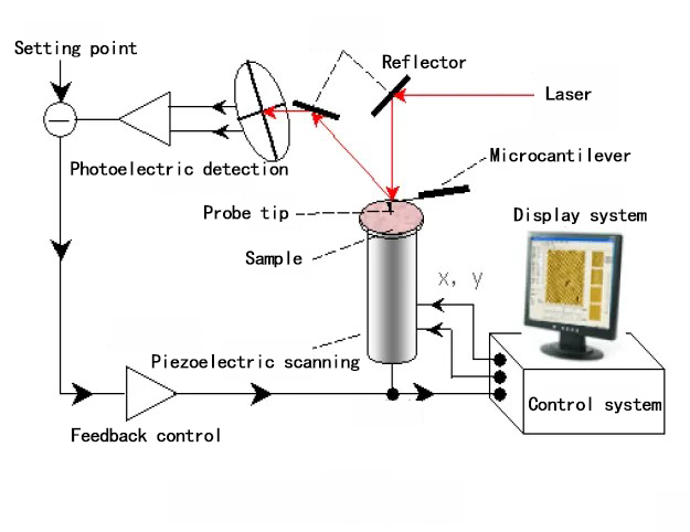
Within an Atomic Force Microscope (AFM) setup, a highly responsive microcantilever is anchored at one extremity, while the opposing end carries a nanoscopic probe that interacts delicately with the specimen’s exterior. Due to the minute repulsive forces between the atoms of the tip and the sample, the cantilever undergoes vertical displacement as it maintains a uniform force during the scanning process. This rhythmic movement effectively maps the equipotential landscape of the tip-sample atomic interactions. Utilizing optical or tunneling current sensing techniques, the spatial variations of the cantilever are recorded at every coordinate, enabling the reconstruction of the sample’s three-dimensional surface morphology.

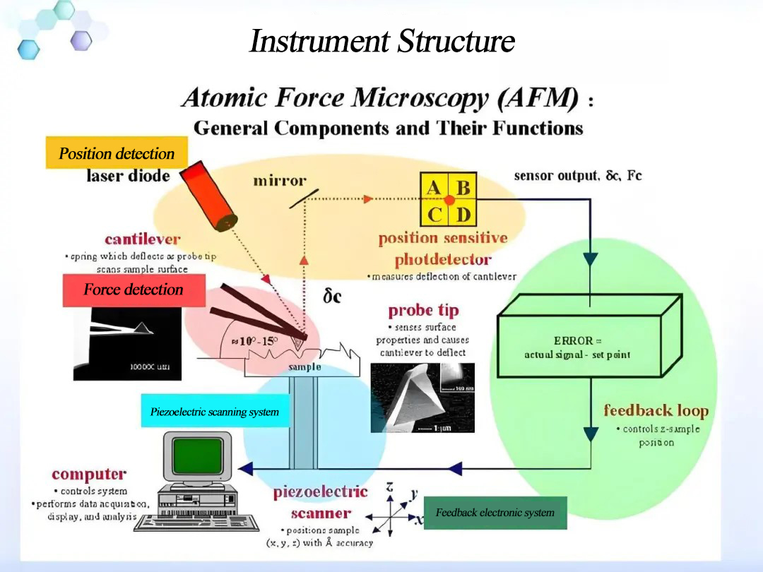
The basic structure of Atomic Force Microscope
The primary components of an atomic force microscope encompass the probe, probe positioning and scanning mechanisms, force detection sections, and feedback control units. The probe material is typically a harder metal, with tungsten wire being a widely used choice. Through processes such as electrochemical etching and focused ion beam milling, probes featuring a smaller tip radius can be produced.

The imaging modes of Atomic Force Microscope
AFM has three basic imaging modes:
● Contact mode: The probe tip is in soft “actual contact” with the sample. As the tip gently scans across the sample surface, the contact force causes the cantilever to bend, thereby obtaining the surface profile of the sample.
● Non-contact mode: In non-contact mode, the tip vibrates above the sample surface without ever coming into contact with it. The detector measures long-range forces such as van der Waals forces and electrostatic forces that do not damage the sample being images.
● Tapping mode: In tapping mode, the tip vibrates at a certain frequency and amplitude above the sample surface, never coming into contact with it. The detector senses changes in the resonance frequency and amplitude of the tip’s forced vibration, thereby obtaining information about the sample’s surface topography.
The instrumental features of Atomic Force Microscope
- High Spatial Resolution: AFM is capable of achieving atomic-level spatial resolution. Under optimal conditions, it can even reveal the arrangement and structure of individual atoms.
- Non-Destructive Measurement: AFM’s measurement process is non-destructive, meaning the sample remains unaltered or undamaged during the process. This is particularly crucial for studying delicate biological samples and soft materials.
- Wide Sample Applicability: AFM can be applied to a broad range of samples, including both conductive and non-conductive materials, as well as samples in solid and liquid environments, at room temperature and low temperatures.
- Versatility: AFM is not limited to topographic imaging; it can also measure mechanical properties (such as hardness and elastic modulus) and characterize electrical properties (such as conductivity and local potential).
- Dynamic and Static Measurements: AFM can perform both dynamic measurements (e.g., tapping mode) and static measurements (e.g., contact mode), making it adaptable to various measurement requirements and sample characteristics.
- Environmental Adaptability: AFM can operate under diverse environmental conditions, including high humidity, high temperature, low temperature, and various chemical atmospheres. This makes it highly valuable in materials science and industrial applications.
- Simple Sample Preparation: Unlike some characterization techniques that require complex sample preparation, AFM typically does not necessitate intricate sample processing.
- Compatibility with Other Techniques: AFM can be combined with other characterization methods, such as Raman spectroscopy and infrared spectroscopy, to provide more comprehensive sample information.
Atomic force microscopy (AFM) is one of the most cutting-edge and powerful characterization techniques in the field of electrochemistry, particularly for observing the SEI film (solid electrolyte interface).
The properties of the SEI film (thickness, uniformity, mechanical strength) directly determine the battery’s cycle life, safety, and rate performance. AFM’s applications in this area are mainly reflected in the following dimensions:
In-situ Dynamic Observation (In-situ AFM): Observing the “Growth Process” of SEI
This is the most significant advantage of AFM in battery research. Using a special in-situ electrochemical cell, scientists can observe in real time the entire process of electrolyte decomposition on the electrode surface and the formation of the SEI film during battery charging and discharging.
- Observation Content: From which sites does the SEI film begin to nucleate? How does it thicken or undergo morphological evolution with increasing cycle number?
- Research Value: Helps optimize the “formation” process. For example, by observing the effect of different additives (such as VC, FEC) on the density of the SEI film, better electrolyte formulations can be screened.
Mechanical Property Characterization: Measuring the “Toughness” of the SEI
The SEI film must not only be able to conduct ions but also be sufficiently strong and tough to withstand the volume expansion/contraction of the electrode material during lithium insertion/extraction.
- Functional Mode: Utilizing Peak Force QNM (Quantitative Nanomechanical Mapping) mode.
- Observations: Measuring the Young’s modulus, adhesion force, and hardness of the SEI film.
- Research Value: If the SEI film is too brittle, cracks will form during electrode expansion, leading to continuous electrolyte consumption and battery capacity decay. AFM can help assess the mechanical stability of the SEI film.
Precise Measurement of Thickness and Roughness
SEI films are typically only a few to tens of nanometers thick and are highly susceptible to environmental influences (e.g., sensitivity to water and oxygen).
- Observation Content: Using nano-scraping technology, AFM can purposefully “scrape away” a small piece of the SEI film, and the precise thickness of the SEI film can be obtained by measuring the depth of the scratch.
- Research Value: Comparing the thickness changes of the SEI film under different states of charge and discharge (SOC) allows for the study of its dissolution and regeneration during cycling.
Conductivity and Potential Distribution (C-AFM & KPFM)
Besides morphology, AFM can be used for other detection functions:
- C-AFM (Conduction Atomic Force Microscopy): Detects the electronic conductivity distribution on the SEI film surface, ensuring it is electronically insulating (preventing continuous electrolyte decomposition).
- KPFM (Kelvin Probe Force Microscopy): Measures surface potential. This helps study the charge distribution on the SEI film surface and understand how ions migrate across the interface.
Real-world research examples
- Graphite Anode: Uses AFM to observe the exfoliation phenomenon between graphite layers at low potentials and how the SEI film covers and inhibits this exfoliation.
- Silicon Anode: Silicon undergoes a huge volume change (approximately 300%) during charging and discharging. Observing the cracking and repair process of its surface SEI film through AFM is a core method for studying the failure mechanism of silicon-carbon anodes.
- Lithium metal anode: Real-time monitoring of lithium dendrite nucleation sites and how the uniformity of the SEI film affects the lithium deposition morphology.
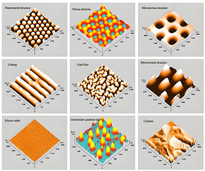
The typical morphology of Atomic Force Microscope
AFM images of materials with large surface to volume ratio

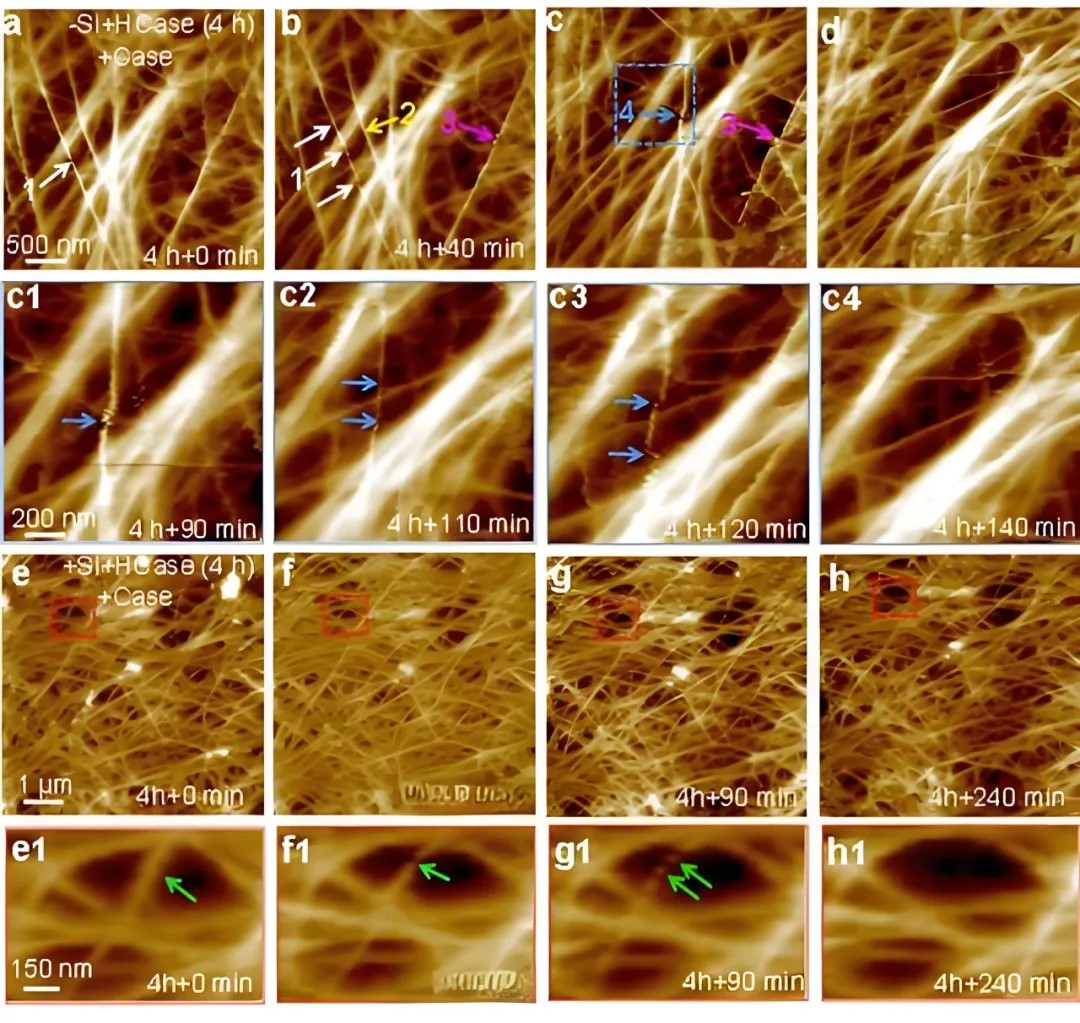
In situ AFM observation of cellulase
About Neware:
Neware was founded in 1998. We are trusted by ATL, BYD, CATL, Tesla, Apple, HUAWEI, SolarEdge, etc. We provide battery testing solutions for testing battery cell, module, pack, supercapacitor, BESS, etc. If you want to do capacity, cycle life, pulse, DCIR, GITT, HPPC, or EV driving simulation test, please feel free to contact us.
If you do battery research or battery materials research, you might be interested in these products:

